DIY high quality USB audio adapter. Parallel DACs Homemade DAC Input Transformer
Igor GUSEV, Andrey MARKITANOV
Gavrila was an audiophile,
Gavrila DACs created ...
Indeed, why don't we make a DAC with our own hands? Is it necessary at all? Certainly! An external converter will be useful, first of all, to owners of CD players released 5 - 10 years ago. The technology of digital sound processing is developing at a rapid pace, and the idea of reviving the sound of an old but beloved device with the help of an external DAC seems very tempting. Secondly, such a device can be of great benefit to those who have an inexpensive model equipped with a digital output - this is a chance to take its sound to a new level.
It's no secret that when creating an inexpensive CD player, the developer is in a tight financial framework: he needs to choose a more decent vehicle, and equip the new product with all sorts of services to the maximum, bring more buttons with a multifunctional indicator to the front panel, etc., otherwise strict laws of the market, the device will not be sold. In a year, as a rule, a new one will appear, which sometimes does not sound better than the old one (and often worse), and so on ad infinitum. And most large firms usually change the entire lineup every spring ...
The allocated funds are usually not enough for a high-quality DAC and the analog part of the circuit, and many manufacturers frankly save on this. There are, however, exceptions to this rule, when such decisions are made intentionally, being an element of the company's technical policy.
For example, the Japanese C.E.S., well known to our audiophiles. puts expensive vehicles with a large number of manual adjustments into its CD2100 and CD3100 models, while using a simple DAC, which obviously does not correspond to the mechanics in terms of class. These devices are positioned by the company as vehicles with a control audio path and are originally designed to work with an external converter. The situation is somewhat different with TEAS VRDS 10 - 25 players. By installing a high-class drive and expensive TDA1547 (DAC 7) DAC chips, the engineers for some reason decided to save on output stages. One Russian company, knowing about this feature of the models, makes an upgrade, replacing the analog part of the circuit.
About authors
Andrey Markitanov, engineer at the Three V sound engineering design bureau from Taganrog. Develops and introduces into production DACs under the Markan brand, a regular participant in Russian Hi-End exhibitions. He loves non-standard solutions, follows the audio fashion, always up to date with the latest achievements in the field of digital circuitry. He knows the pinouts of many Crystal, Burr-Brown and Philips chips from memory.
A bit of theory
So, it's decided - we make a DAC. Before we begin to consider the scheme, it is useful to decipher some common abbreviations:
S/PDIF (Sony/Philips Digital Interface Format)- standard for digital transmission of audio data between devices (asynchronous interface with self-synchronization). There is also an optical version of TosLink (from the words Toshiba and Link). Almost all models of inexpensive CD players are equipped with this interface, but now it is considered obsolete. There are more advanced interfaces used in expensive devices, but we won't talk about them yet.
DAC (DAC)- digital-to-analog converter.
IIS (InterIC Signal bus)- a standard for a synchronous interface between circuit elements within the same device.
PLL (Phase Locked Loop)- phase locked loop system.
Emphasis- predictions.
Currently, there are two completely different ways of digital-to-analogue conversion for the CD Audio format: single-bit and multi-bit. Without going into the details of each of them, we note that the vast majority of expensive DAC models use multi-bit conversion. Why expensive? A decent implementation of this option requires a high-quality multi-channel power supply, a complex procedure for setting output filters, in some models it is done manually, and in developed countries the work of a qualified specialist cannot be cheap.
However, single-bit converters also have a lot of fans, because. they have a peculiar sound delivery character, some features of which are difficult to achieve with existing multi-bit technology. These include the higher linearity of single-bit DACs at low signal levels, and hence better microdynamics, distinct detailed sound. In turn, the argument of supporters of multi-bit DACs is a stronger emotional impact on the listener, the scale and openness of the sound, the so-called. "drive" and "ches", which is especially appreciated by rock lovers.
In theory, single-bit DACs require a very high clock speed to work flawlessly. In our case, i.e. 16 bits and 44.1 kHz, it should be around 2.9 GHz, which is absolutely unacceptable value from a technical point of view. With the help of mathematical tricks and all kinds of recalculations, it can be reduced to acceptable values within a few tens of megahertz. Apparently, this explains some of the features of the sound of one-bit DACs. So which one is better? We will describe both options, and which one to choose - decide for yourself.
The main thing that guided us when developing the circuit was its extreme simplicity, which allows us to understand the idea and implement it in a specific design, even for an audiophile who is not experienced in digital technology. Nevertheless, the described DAC is able to significantly improve the sound of a budget device equipped with a coaxial digital output. If your player does not have one, then it will be easy to organize it yourself. To do this, in most cases, it is enough to install an RCA connector on the back wall and solder its signal lobe to the appropriate place on the board. As a rule, the basic version of the motherboard is made for several models at once, only it is “stuffed” in different ways, and there must be a place on it for soldering the digital output jack. If this is not the case, you will have to look for a diagram of the device - in authorized service centers, on radio markets or on the Internet. In the future, this layout can serve as the object of efforts to further improve it and allow, finally, to achieve a "gentle haze over a clean image."
Almost all devices of this purpose are built on a similar element base, the choice of elements for the developer is not so wide. Among those available in Russia, we will name Burr-Brown, Crystal Semiconductors, Analog Devices, Philips microcircuits. Of the S / PDIF signal receivers, CS8412, CS8414, CS8420 from Crystal Semiconductors, DIR1700 from Burr-Brown, AD1892 from Analog Devices are more or less available at affordable prices. The choice of DACs themselves is somewhat wider, but in our case, the use of CS4328, CS4329, CS4390 with delta-sigma conversion seems to be optimal, they most fully meet the quality / price criterion. Burr-Brown's $96 multi-bit PCM63 multi-bit chips, or more recent PCM1702s, which are widely used in the High End, also require certain types of digital filters, which are also not cheap.
So, we choose Crystal Semiconductors products, and the documentation for microcircuits with their detailed description, pinout and status tables can be downloaded from the site www.crystal.com.
| Converter details | ||
|---|---|---|
| resistance | ||
| R1 | 220 | 1/4w |
| R2 | 75 | 1/4w |
| R3 | 2k | 1/4w |
| R4 - R7 | 1k | 1/4w |
| R8, R9 | 470k | 1/4w carbon |
| Capacitors | ||
| C1 | 1.0uF | ceramics |
| C2, C4, C8, C9 | 1000uF x 6.3V | oxide |
| C3, C5, C7, C120 | 1 uF | ceramics |
| C6 | 0.047uF | ceramics |
| C10, C11 | 1.0uF | K40-U9 (paper) |
| Semiconductors | ||
| VD1 | AL309 | red LED |
| VT1 | KT3102A | npn transistor |
| U1 | CS8412 | digital signal receiver |
| U2 | 74HC86 | TTL buffer |
| U3 | CS4390 | DAC |
Let's go to the diagram
So, the question remains: which scheme to choose? As already mentioned, it should be uncomplicated, easy to repeat and have sufficient potential for sound quality. It also seems mandatory to have an absolute phase switch, which will make it possible to better match the DAC with the rest of the audio path elements. Here is the best, in our opinion, option: a CS8412 digital receiver and a CS4390 single-bit DAC costing about $7 per case (it's better to try to find a DIP option, this will noticeably facilitate installation). This DAC is used in the famous Meridian 508.24 player model and is still considered the best by Crystal. The multi-bit version uses the Philips TDA1543 chip. The circuit of a one-bit converter looks like this:
Resistors R1-R7 are small-sized, of any type, but R8 and R9 are better to take the BC series or imported carbon ones. Electrolytic capacitors C2, C4, C8, C9 must be rated at least 1000 microfarads with an operating voltage of 6.3 - 10 V. Capacitors C1, C3, C5, C6, C7 are ceramic. C10, C11 it is desirable to use K40-U9 or MBHCH (paper in oil), but film K77, K71, K73 (listed in descending order of priority) are also suitable. Transformer T1 - for digital audio, getting it is not a problem. You can try to use a transformer from a faulty computer network card. The diagram does not show the power connection of the U2 microcircuit, the minus is supplied to the 7th leg, and the plus to the 14th.
To maximize the sound potential of the circuit, it is advisable to adhere to the following installation rules. All connections to the common wire (marked with the GND icon) are best made at one point, for example, at pin 7 of the U2 chip. The greatest attention should be paid to the digital signal input node, which includes the input jack, elements C1, T1, R2 and pins 9,10 of the U1 chip.
It is necessary to use the shortest possible connections and leads of the components. The same applies to a node consisting of elements R5, C6 and pins 20, 21 of the U1 chip. Electrolytic capacitors with appropriate ceramic shunts should be installed in close proximity to the power supply pins of the microcircuits and connected to them with conductors of a minimum length. The diagram does not show another electrolyte and a ceramic capacitor, which are connected directly to power pins 7 and 14 of the U2 chip. It is also necessary to interconnect pins 1, 2, 4, 5, 7, 9, 10 of the U2 chip.
After gaining some experience, you will be able to select by ear the size and type of electrolytic and ceramic capacitors that are in power circuits in each specific area.
Now a few words about the operation of the circuit itself. LED D1 serves to indicate that the digital receiver U1 captures the signal from the transport and the presence of reading errors. During normal playback, it should not glow. Contacts S1 switch the absolute phase of the signal at the output, this is similar to changing the polarity of speaker cables. By changing the phasing, you can notice how it affects the sound of the entire path. The DAC also has a de-emphasis correction circuit (pin 2/U3), and although there are not many discs with pre-emphasis released, such a function can come in handy.
Now for the output circuits. Direct connection of the DAC chip to the output only through coupling capacitors is possible, since the CS4390 chip already has a built-in analog filter and even an output buffer. The CS4329 and CS4327 chips are built on a similar principle, the CS4328 DAC also had a good analog part. If you know how to make high-quality low-pass filters and matching stages, you should try your hand at the magnificent CS4303 microcircuit, which has a digital signal at the output and makes it possible to build a great-sounding device if, for example, you connect a kenotron-powered tube buffer to it.
But back to our CS4390. The principle of building one-bit DACs assumes the presence of significant amplitude impulse noise in the internal power circuits. To reduce their influence on the output signal, the output of such DACs is almost always done according to a differential circuit. In this case, we are not interested in record signal-to-noise ratios, so we use only one output for each channel, which avoids the use of additional analog stages that can negatively affect the sound. The signal amplitude at the output jacks is quite sufficient for normal operation, and the built-in buffer copes well with such loads as interconnect cable and amplifier input impedance.
Now let's talk about the power of our device. Sound is just a modulated power supply and nothing else. As is the food, so is the sound. We will try to pay special attention to this issue. The initial version of the power stabilizer for our device is shown in Fig. 2

The advantages of this scheme are its simplicity and clarity. With a common rectifier, different stabilizers are used for the digital and analog parts of the circuit - this is a must. Between themselves, they are decoupled at the input by a filter consisting of C1, L1, C2, C3. Instead of five-volt 7805 regulators, it is better to put adjustable LM317 with appropriate resistive dividers in the control output circuit. The calculation of resistance values can be found in any reference book on linear microcircuits. Compared to the 7805, LM317s have a wider frequency range (don't forget that not only direct current flows through the power circuits, but also a broadband digital signal), less internal noise and a quieter response to a pulsed load. The fact is that when impulse noise appears (and they are apparently invisible in terms of power!) The stabilization circuit, covered by deep negative feedback (it is necessary to obtain a high stabilization coefficient and low output resistance), tries to compensate for it. As expected for circuits with OOS, a damped oscillatory process occurs, on which newly arrived interference is superimposed, and as a result, the output voltage constantly jumps up and down. It follows from this that it is desirable to use stabilizers on discrete elements that do not contain an OS to power digital circuits. Of course, in this case, the output impedance of the source will be much higher, so the entire responsibility for combating impulse noise is shifted to shunt capacitors, which do a good job of this task, and this has a beneficial effect on the sound. In addition, the need to use a separate stabilizer for each power output of digital microcircuits, along with power decoupling elements (similar to L1, C2, C3 in Fig. 2), clearly emerges.
In Markan DACs, this is done, and the filter with additional suppression of digital noise and the rectifier work from a separate winding of the mains transformer, and different transformers are even used for additional decoupling of the digital and analog parts of the circuit. The same is being done to further improve our DAC, although the circuit in Fig. 2 can be used to begin with, it will provide an initial level of sound quality. In the rectifier, it is better to use fast Schottky diodes.
Multi-bit variant of the scheme
Typically, multi-bit DACs require several voltage sources of different polarity and a considerable number of additional discrete elements for their operation. Among the wide variety of microcircuits, we will opt for the Philips TDA1543. This DAC is a "budget" version of the excellent TDA 1541 chip, costs a penny and is available at retail in our country.
The TDA 1541 chip was used in the Arcam Alpha 5 CD player, which at one time collected many prizes, although it was also strongly scolded - antediluvian DAC, strong interference, but how it sounds! This chip is also still used in Naim turntables. TDA1543 is great for our purposes, because. it requires only one +5V power supply and requires no additional parts. We unsolder the CS4390 from the digital receiver and connect the TDA 1543 in its place in accordance with the diagram in fig. 3.
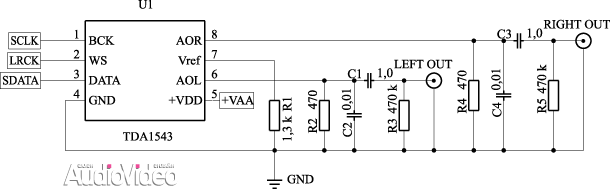
A few additional clarifications need to be made here. All multi-bit DACs have a current output, and there are several circuit designs for converting the signal to voltage. The most common is an operational amplifier connected with an inverting input to the output of the DAC. The current-voltage conversion is carried out at the expense of the OS covering it. In theory, it works great, and this approach is considered a classic - it can be found in the recommended options for including any multi-bit DAC. But if we talk about sound, then everything is not so simple. To implement this method in practice, very high-quality op-amps with good speed characteristics are required, for example, AD811 or AD817, which cost more than $5 apiece. Therefore, in budget designs, they often act differently: they simply connect an ordinary resistor to the DAC output, and the current passing through it will create a voltage drop, i.e. complete signal. The value of this voltage will be directly proportional to the value of the resistor and the current flowing through it. Despite the apparent simplicity and elegance of this method, it has not yet been widely used by manufacturers of expensive equipment, because also has many pitfalls. The main problem is that the current output of DACs does not provide for the presence of voltage on it and is usually protected by diodes connected back-to-back and introduce significant distortions into the signal received at the resistor. Among well-known manufacturers who nevertheless decided on such a method, Kondo should be singled out, which puts a resistor wound with silver wire in its M-100DAC. Obviously, it has a very small resistance and the amplitude of the output signal is also very small. To obtain a standard amplitude, several tube amplification stages are used. Another well-known company with an unconventional approach to the issue of current-to-voltage conversion is Audio Note. In her DACs, she uses a transformer for this purpose, in which the current passing through the primary winding causes a magnetic flux, leading to the appearance of a signal voltage on the secondary winding. The same principle is implemented in some DACs of the Markan series.
But back to the TDA 1543. It seems that the developers of this microcircuit, for some reason, did not install protective diodes at the output. This opens up the prospect of using a resistor current-to-voltage converter. The resistances R2 and R4 in fig. 3 is just for that. With the indicated ratings, the output signal amplitude is about 1 V, which is quite enough for direct connection of the DAC to a power amplifier. It should be noted that the load capacity of our circuit is not very high, and under unfavorable conditions (high capacitance of the interconnect cable, low input impedance of the power amplifier, etc.), the sound can be slightly clamped in the dynamics and “smeared”. In this case, the output buffer will help, the scheme and design of which you can choose from a variety of existing options. It may happen that in some manufactured versions of the TDA 1543 microcircuit, protective diodes are still installed (although there is no such information in the specifications, and we also did not come across specific instances). In this case, it will be possible to remove a signal with an amplitude of not more than 0.2 V from it, and you will have to use an output amplifier. To do this, it is necessary to reduce the value of resistors R2 and R4 by 5 times. Capacitors C2 and C4 in fig. 3 form a first-order filter that removes RF noise from the analog signal and generates the desired frequency response in the upper part of the range.
Many DAC designs use digital filters, which greatly simplifies the task of the developer when designing the analog part, but at the same time, the digital filter bears most of the responsibility for the final sound of the device. Recently, they have been abandoned, since a competent analog filter effectively suppresses high-frequency noise and does not have such a detrimental effect on musicality. This is exactly what is done in Markan DACs, which use a conventional third-order filter with a linear phase response, made on LC elements. In our scheme in Fig. 3, for simplicity, a first-order analog filter is used, which in most cases is quite enough, especially if you use a tube power amplifier, and even without feedback. If your equipment is transistorized, then it is quite possible that you will have to increase the filter order (however, do not overdo it, too steep a circuit will definitely worsen the sound). You will find the corresponding schemes and formulas for calculation in any decent amateur radio handbook.
Please note that resistors R2, R4 and capacitors C2, C4 are located exactly in the place where the analog sound originates. High End starts from here and, as they say, "further everywhere." The quality of these elements (especially resistors) will greatly affect the sound of the entire device. Resistors must be installed with carbon VS, ULI or boron-carbon BLP (after selecting them for the same resistance using an ohmmeter), the use of imported exotics is also welcome. Capacitors are allowed any type of the above. All connections must be of minimum length. Of course, quality output connectors are also needed.
What did we get?
I used to sing verses badly,
wheezed, yelled and lied to the motive ...(J.K. Jerome, "Three in a Boat,
except for the dog)
I'm not too lazy to remind you that before turning on the device for the first time, you must carefully check the entire installation. In this case, the volume control of the amplifier must be set to the minimum position and the volume should be gradually increased if there is no interference, whistle and background at the output. Be careful and careful!
In general, single-bit DACs are characterized by a very soft, pleasant sound, with an abundance of fine details. It seems that they throw all their sound potential to the aid of the soloist, pushing the other participants in the musical work somewhere into the background. Large orchestras are somewhat "reduced" in terms of the composition of the musicians, the power and scale of their sound suffer. Multi-bit DACs pay equal attention to all participants in the musical action, without alienating or highlighting any of them. The dynamic range is wider, the sound is more even, but at the same time somewhat more detached.
For example, when playing the well-known song “I Put A Spell on You” performed by Creedence Clearwater Revival through a multi-bit DAC, its energy is perfectly conveyed, the powerful flow of emotions simply fascinates, the intention of its creators becomes clear, we acutely feel what they wanted to tell us. Small details are somewhat blurred, but against the background of the dominant characteristics of such a sound delivery described above, this does not seem to be a serious drawback. When playing the same song through a one-bit DAC, the picture is somewhat different: the sound is not so large-scale, the stage is somewhat pushed back, but the details of the sound production, small touches are perfectly audible. The moment is well conveyed when the musician brings the guitar closer to the amp, achieving a slight self-excitation of the amplifier. But when listening to Elvis Presley, all the richness of his voice is perfectly revealed. It is clearly seen how it changed with age, the emotional impact on the listener is also strong, and the accompaniment, somewhat relegated to the background, organically fits into the overall picture.
So the choice of the type of DAC is up to you, both options have both strengths and weaknesses, the truth, of course, lies somewhere in the middle. Despite the simplicity, the sonic potential of the described circuits is quite high, and if the above recommendations are creatively implemented, the final results should not disappoint you. We wish you success!
Questions from the schema designer
Being a "happy" owner of an integrated sound subsystem, I still dreamed of a good sound card, and I could not even think that I could make it myself at home. Once, surfing the World Wide Web, I came across a description of a sound card with a USB interface on a Burr-Brown PCM2702 chip and, looking at the prices of companies selling radio components, I realized that this was not for us yet - no one knew anything about it. Later, my computer was built in a small microATX case that didn't even have room for an old Creative Audigy2 ZS. I had to look for something small and preferably external with a USB interface. And then again I came across the PCM2702 chip, which was already actively used and praised for the quality of music playback - with the right circuitry, the sound was much more pleasant than that of the same Audigy2 ZS. Again, a search for prices, and lo and behold, the desired microcircuit is available at a price of about 18 "enemy money". As a result, a couple of chips were ordered for experiments, so to speak, to listen to what the bourgeois “CABuilders” had piled up there.
So, what kind of beast is this PCM2702 controller from the legendary company Burr-Brown, which won the hearts of audiophiles around the world with its top solutions? I wonder what the budget solution is capable of?
According to the technical documentation for the microcircuit (pcm2702.pdf), we have a digital-to-analog converter (digital-to-analog converter - DAC) with a USB interface with the following characteristics:
- Bit depth 16 bits;
- Sampling rate 32 kHz, 44.1 kHz and 48 kHz;
- Dynamic range 100 dB;
- Signal-to-noise ratio 105 dB;
- The level of non-linear distortion 0.002%;
- USB1.1 interface;
- Digital filter with 8x oversampling;
- Works with standard USB audio device driver.
Now about the device itself. To begin with, a simple version was assembled according to the scheme recommended by the manufacturer with minor changes in nutrition. It turned out a small “zvukovuha” powered by USB.

But such a device was not complete and required an external amplifier, and the headphones could not be shaken normally. Later, the motherboard was replaced with another one with a normal HAD codec and good board layout. The audio path was devoid of extraneous noise and rustles, and the quality of the output signal was no worse than that of the PCM2702. And, probably, these lines did not exist, if such a box had not caught my eye:


This is a passive cooling system for HDD, but for me, first of all, this is a chic case for radio equipment. I immediately realized that something would be assembled in it, for example, a sound card with an amplifier, since there should be no problems with cooling. I thought a lot about the circuitry of the device. On the one hand, I wanted high quality, but on the other hand, I didn't want to pay more than ready-made sound cards from Creative cost. The main question arose about the LPF and the headphone amplifier, because high-quality components for these purposes can cost as much as the PCM2702 itself, or even more. For example, high-quality LPF op-amps, OPA2132 and OPA627, cost about $10 and $35, respectively. Headphone amplifier chips - AD815 or TPA6120, I did not find at all in the price lists, moreover, their prices are not small either.
But there is no harm without good, and I found on the Web a simple and high-quality LPF circuit on transistors, the author of which claimed decent sound, even no worse than expensive operational amplifiers. Decided to try. As a headphone amplifier, I installed the LM1876 microcircuit - the younger two-channel "sister" of the legendary LM3886 with the same sound but less power. This microcircuit allows, by increasing the gain, to connect speakers.
The result is such a scheme - USB-DAC_PCM2702_Sch.pdf, drawing of a printed circuit board - USB-DAC_PCM2702_Pcb.pdf in mirror image for transferring the image by laser-ironing method to copper foil, the so-called LUT (you can read more on the Internet), a drawing of the arrangement of elements and jumpers on the board, as well as the connection diagram of the volume control - USB-DAC_PCM2702.pdf.
The assembled board looks like this:


I’ll tell you a little about how it all works, if suddenly there are those who want to assemble such a unit. The PCM2702 switching circuit is standard - LPF is a Sallen-Kay filter, a second-order low-pass filter with unity gain, since the active element works as a follower, an emitter or source follower can be used without problems. There is already room for experimentation. You can choose the type of transistors that you like best in terms of sound - I, testing from what was available, settled on a KT3102E in a metal case (VT3, VT4 - see the USB-DAC_PCM2702_Sch diagram). The filter elements most affect the sound, especially capacitors C25, C26, C31, C32. Experts in this business recommend installing WIMA FKP2 film capacitors, FSC foil polystyrene or Soviet PM. But there was nothing normal in stock and I had to put what was, and only then I changed it to the best. The board provides contact pads for both output and SMD capacitors. Resistors R9, R10, R11, R12 need identical pairs, for which we take resistors with an accuracy of 1% or select pairs with a multimeter. I selected from several dozen resistors with an accuracy of 5%, since there was no time to wait until they brought them with an accuracy of 1%. The values of resistors and capacitors can be selected according to the sound, as you like, but the only condition is that the pair must be the same so that each channel does not sing in its own way.
The circuit provides for disabling the PCM2702 analog power supply and the filter output from the X5, X6 connectors if the USB cable is not connected to the X1 connector. This is to ensure that the filter's low output impedance does not interfere with the signal fed to these jacks when using the device as a headphone amplifier. When connected, analog power to the DAC is supplied through transistor VT2, which is controlled by transistor VT1, if there is voltage at the USB connector, then both transistors are open. The filter outputs are connected to the rear panel connectors via relay K1, which is also powered by USB. I used the relay V23079-A1001-B301 from AXICOM. If there is no such relay, then instead of it you can put a conventional switch with two contact groups. Instead of the transistor VT2, you can also put a switch, and you don’t need to solder all the elements responsible for switching the power supply, it is only desirable to switch the USB power itself through the same switch.
The amplifier and the analog part are powered by an external power supply with a voltage of 12-15 V and 0.5 A AC, connected via the X2 connector on the rear panel.

The power supply itself was made from a conventional stabilized 12 V 0.5 A PSU by throwing away everything superfluous.

In the amplifier, you also need to select resistors R15-R18 in pairs, which set the gain (left channel Cool = R17/R15, Cup = R18/R16). If you do not plan to use headphones, then you can connect speakers, then you need to reduce the resistance of resistors R15, R16 to 4.7-10 kOhm, you can slightly increase the resistance R17, R18. Thus, it will be possible to obtain a nominal output power of about 2 x 5 watts. If you power the D6 chip with a voltage of +/- 20 ... 25 V, which is taken immediately after the rectifier from the capacitors C6, C7, you can get a maximum output power of 2 x 18 W, but for this you will need to put the diodes VD2, VD3 on a current of at least 3A , replace fuse F2 with a current of at least 3A, double the capacitance of condensates C6, C7 and use a transformer in the power supply of greater power, approximately 16 V 4 A AC.
All SMD resistors, resistors R20, R22 size 1206, resistors R13, R14 size 2010 can be replaced by jumpers, all other resistors size 0805. All SMD ceramic capacitors size 0805, all electrolytic capacitors with a maximum operating temperature of 105 ° C and low internal resistance , with an operating voltage of 16 V, capacitors C6, C7 with a maximum operating voltage of 25-35 V. Most of the connectors are soldered from old equipment, I can’t say for sure, be guided by appearance. The volume control resistor is connected with a two-wire shielded wire, two signal channels and ground on the screen, a resistor of unknown Chinese origin with a resistance of 20 kOhm of group B (with an exponential dependence of resistance on the angle of rotation of the knob).
I also want to tell you a little about how to solder microcircuits in such a small package. Some mistakenly believe that such microcircuits need to be soldered with low power soldering irons and a thin tip. It's very fun to watch when people sharpen the sting like an awl and try to solder each leg individually. In fact, everything is easy and simple. To begin with, we install the microcircuit in the desired position, hold it with our hand or fix it with glue, solder one of the extreme terminals, then center it, if necessary, and solder the opposite terminal. If several conclusions are soldered together, then this is not scary. The soldering iron is taken with a power of 30-50 W with a tinned, freshly sharpened tip at an angle of about 45 °, and we do not spare flux or rosin. The flux is preferably not active, otherwise you will have to wash the board very carefully trying to wash it out from under the microcircuit. We warm up all the legs with a small drop of solder, starting from one edge and gradually, as it warms up, move the soldering iron towards the non-soldered leads, driving excess solder onto them, while the board can be held at an angle so that the solder flows down under gravity itself. If there is not enough solder, take a little more, if there is a lot, then with the help of a rag we remove all the solder that is on the tip of the soldering iron, and without sparing the flux, we remove the excess from the microcircuit pins. Thus, if the board is normally etched, well cleaned and degreased, then the soldering takes place within 1-3 minutes and it turns out to be clean, beautiful and uniform, which can be seen on my board. But for greater certainty, I recommend practicing on burned boards from various computer equipment with microcircuits that have approximately the same pin pitch.
I recommend that you first do not solder the D2 and D6 chips and elements that may interfere with their installation. First of all, it is necessary to solder the nodes responsible for power supply, ring the power circuits for a short circuit, connect to the USB port and apply 14 V AC from the power supply to X2. Future outputs of stabilizer microcircuits should have the following voltages:
- D1: +3.3V;
- D3: +12V;
- D4: -12V;
- D5: +5 V.
When connecting the PCM2702 to the computer for the first time, the system finds a new device - USB Speakers Burr-Brown Japan PCM2702.

After automatically installing the driver in Device Manager, a new device will appear - USB Speakers. This means that everything works as it should and you can turn on music, video, or even run games.

The system automatically transmits sound to the PCM2702 chip when it is connected to a computer and returns to its original state when the board is turned off, to resume playback, you just need to restart the desired program. The volume is controlled by the standard Windows volume control. I checked the board's performance only under Windows XP SP2.
A little about assembling the entire device into a case. The hardest part is setting the volume control's variable resistor. The front panel is attached to the chassis by a ledge that runs along the back side of the panel and has a rather serious thickness. This ledge must be cut with a hacksaw or milling machine in the place where the volume control will be attached, but you need to be very careful, as you can scratch the aluminum coating, which will make the panel lose its attractiveness. Then we drill a hole for mounting the resistor, the place for which we estimate according to the position of the handle, which will be put on this same resistor. On the front side, we slightly remove the ribs near the hole so that the nut gets the threads on the base of the resistor. There is one more problem - the center of the panel does not coincide with the center of the internal chamber of the chassis, and the volume control resistor rests against the case. I had to raise the panel by 2-3 mm, for which I cut off the corner of the protrusion for fastening with a dremel.
I will not describe in detail all the actions with the panel and chassis. Those who can make such a device themselves will understand everything from the photographs. Where holes were drilled and threaded, 2 washers were placed under the panel during installation near each screw to raise it by 2 mm. Holes are also drilled in the chassis and threads are cut for mounting the board. Microcircuits D3, D4 and D6 are pressed to the chassis with M2.5 screws, while D4 and D6 must be isolated from the panel using a mica plate or other heat-conducting dielectric or chips with an insulated case, like D6 in my case, should be used. The back panel is made of a plastic plug from the system unit. All this can be seen in more detail in the photo.
Most parallel DAC circuits are based on the summation of currents, the strength of each of which is proportional to the weight of the digital bit, and only the currents of the bits whose values are equal to 1 should be summed. Let, for example, it is required to convert a binary four-bit code into an analog current signal. For the fourth, most significant digit (SZR), the weight will be equal to 2 3 =8, for the third digit - 2 2 =4, for the second - 2 1 =2 and for the junior (MSR) - 2 0 =1. If the weight of the MZR I MZR \u003d 1 mA, then I SZR = 8 mA, and the maximum output current of the converter I out.max =15 mA and corresponds to code 1111 2 . It is clear that the code 1001 2 , for example, will correspond to I out = 9 mA, etc. Therefore, it is required to build a circuit that provides generation and switching according to the given laws of exact weight currents. The simplest circuit that implements this principle is shown in Fig. 3.
The resistances of the resistors are chosen so that when the keys are closed, a current flows through them corresponding to the weight of the discharge. The key must be closed when the corresponding bit of the input word is equal to one. The output current is given by

With a high DAC capacity, the current-setting resistors must be matched with high accuracy. The most stringent accuracy requirements are imposed on high-order resistors, since the spread of currents in them should not exceed the current of the least significant level. Therefore, the spread of resistance in k-th digit must be less than
D R /R=2 –k
It follows from this condition that the spread of the resistance of the resistor, for example, in the fourth digit should not exceed 3%, and in the 10th digit - 0.05%, etc.
The considered scheme, for all its simplicity, has a whole bunch of shortcomings. Firstly, for different input codes, the current drawn from the reference voltage source (REF) will be different, and this will affect the value of the output voltage of the REF. Secondly, the resistance values of weight resistors can differ by thousands of times, and this makes it very difficult to implement these resistors in semiconductor ICs. In addition, the resistance of high-order resistors in multi-bit DACs can be commensurate with the resistance of a closed key, and this will lead to a conversion error. Thirdly, in this scheme, a significant voltage is applied to the open switches, which complicates their construction.
These shortcomings are eliminated in the AD7520 DAC circuit (domestic analogue 572PA1), developed by Analog Devices in 1973, which is currently essentially an industrial standard (many serial DAC models are made according to it). This scheme is shown in fig. 4. MOS transistors are used as keys here.

Rice. 4. DAC circuit with switches and constant impedance matrix
In this scheme, the setting of the weighting coefficients of the converter steps is carried out by successively dividing the reference voltage using a constant impedance resistive matrix. The main element of such a matrix is a voltage divider (Fig. 5), which must satisfy the following condition: if it is loaded with resistance R n, then its input impedance R in must also take the value R n. Circuit weakening factor a = U 2 /U 1 at this load should have a given value. When these conditions are met, we obtain the following expressions for the resistances:
in accordance with Fig.4.
Since in any position of the switches S k they connect the lower terminals of the resistors to a common circuit bus, the reference voltage source is loaded with a constant input resistance R in = R. This ensures that the reference voltage remains unchanged for any DAC input code.
According to fig. 4, the output currents of the circuit are determined by the relationships
| (8) |
| (9) |
and input current
| (10) |
Since the lower terminals of resistors 2 R matrices in any state of switches S k are connected to a common circuit bus through the low resistance of closed switches, the voltages on the switches are always small, within a few millivolts. This simplifies the construction of switches and their control circuits and allows the use of a reference voltage from a wide range, including different polarity. Since the output current of the DAC depends on U op linearly (see (8)), converters of this type can be used to multiply an analog signal (by feeding it to the reference voltage input) by a digital code. These DACs are called multiplying(MDAC).
The accuracy of this circuit is reduced by the fact that for DACs with a high bit depth, it is necessary to match the resistances R 0 keys with discharge currents. This is especially important for high order keys. For example, in the 10-bit AD7520 DAC, the key MOSFETs of the six most significant bits are made different in area and their resistance R 0 rises according to the binary code (20, 40, 80, ... , 640 ohms). In this way, the voltage drops on the switches of the first six digits are equalized (up to 10 mV), which ensures the monotonicity and linearity of the DAC transient response. The 12-bit DAC 572PA2 has differential non-linearity up to 0.025% (1 LSM).
DACs based on MOS switches have a relatively low performance due to the large input capacitance of MOS switches. The same 572PA2 has a settling time for the output current when changing the input code from 000...0 to 111...1, equal to 15 µs. Burr-Braun's 12-bit DAC7611 has a 10µs settling time. At the same time, DACs based on MOS switches have a minimum power consumption. The same DAC7611 consumes only 2.5 mW. Recently, DAC models of the type discussed above have appeared with higher speed. For example, the 12-bit AD7943 has a current settling time of 0.6 µs and a power consumption of only 25 µW. Low self-consumption allows these micro-power DACs to be powered directly from the reference voltage source. At the same time, they may not even have an output for connecting an ION, for example, AD5321.
DAC on current sources
DACs on current sources have higher accuracy. In contrast to the previous version, in which the weight currents are generated by relatively low resistance resistors and, as a result, depend on the resistance of the switches and the load, in this case, the weight currents are provided by transistor current sources with a high dynamic resistance. A simplified diagram of the DAC on current sources is shown in fig. 6.

Rice. 6. DAC circuit on current sources
Weight currents are formed using a resistive matrix. The potentials of the bases of the transistors are the same, and so that the potentials of the emitters of all transistors are equal, the areas of their emitters are made different in accordance with the weighting factors. The right resistor of the matrix is not connected to a common bus, as in the diagram in Fig. 4, but to two identical transistors connected in parallel VT 0 and VT n, as a result of which the current through VT 0 is equal to half the current through VT 1 . The input voltage for the resistive matrix is created using the reference transistor VT op and operational amplifier OU1, the output voltage of which is set so that the collector current of the transistor VT op takes on a value I op. Output current for N-bit DAC.
| (11) |
Typical examples of DACs on current switches with bipolar transistors as keys are a 12-bit 594PA1 with a settling time of 3.5 µs and a linearity error of no more than 0.012% and a 12-bit AD565 with a settling time of 0.2 µs with the same linearity error. Even faster is the AD668, which has a 90 ns settling time and the same linearity error. Of the new developments, we can note the 14-bit AD9764 with a settling time of 35 ns and a linearity error of no more than 0.01%.
as current switches S k often used bipolar differential stages in which the transistors are active. This reduces the settling time to a few nanoseconds. The circuit of the current switch on differential amplifiers is shown in fig. 7.

Differential stages VT 1 -VT 3 and VT "1 - VT" 3 are formed from standard ESL valves. Current I k flowing through the collector terminal of the output emitter follower is the output current of the cell. If the digital input D k a high-level voltage is applied, then the transistor VT 3 opens, and the transistor VT "3 closes. The output current is determined by the expression

The accuracy is greatly improved if the resistor R e replace with a direct current source, as in the circuit in fig. 6. Due to the symmetry of the circuit, it is possible to form two output currents - direct and inverse. The fastest models of these DACs have ESL input levels. An example is the 12-bit MAX555, which has a 4 ns settling time to 0.1%. Since the output signals of these DACs capture the RF range, they have an output impedance of 50 or 75 ohms, which must be matched to the characteristic impedance of the cable connected to the output of the converter.
Formation of the output signal in the form of voltage
There are several ways to generate the output voltage for a DAC with the summation of weight currents. Two of them are shown in Fig. 8.

Rice. 8. Formation of voltage on the current output of the DAC
On fig. 8a shows a circuit with a current-to-voltage converter on an operational amplifier (op-amp). This circuit is suitable for all current output DACs. Since the film resistors that determine the weight currents of the DAC have a significant temperature coefficient of resistance, the feedback resistor R OS should be made on a DAC chip and in the same technological process that is usually done. This makes it possible to reduce the temperature instability of the transducer by a factor of 300...400.
For a DAC on MOS switches, taking into account (8), the output voltage of the circuit in fig. 8a.
![]()
Usually the resistance of the feedback resistor R oc = R. In this case
| (12) |
Most DAC models have significant output capacitance. For example, AD7520 with MOS keys, depending on the input code WITH the output is 30 ... 120 pF, for AD565A with current sources WITH vy = 25 pF. This capacitance, together with the output impedance of the DAC and the resistor R oc creates an additional pole in the frequency response of the op-amp feedback loop, which can cause self-excitation instability. This is especially dangerous for DACs with MOS switches with a zero input code. At R os = 10 kΩ, the frequency of the second pole will be about 100 kHz at 100% feedback depth. In this case, an amplifier whose unity gain frequency is f t exceeds 500 kHz, will have clearly insufficient stability margins. To maintain stability, you can connect in parallel with a resistor R os capacitor WITH to, the capacity of which in the first approximation can be taken equal to WITH out. For more precise selection WITH It is necessary to carry out a complete analysis of the stability of the circuit, taking into account the properties of a particular op-amp. These measures degrade the performance of the circuit so seriously that a paradoxical situation arises: to maintain the high performance of even an inexpensive DAC, a relatively expensive high-speed (with a short settling time) op amp may be required.
Early models of DACs with MOS switches (AD7520, 572PA1, etc.) allow a negative voltage on the switches not exceeding 0.7 V, therefore, to protect the switches, a Schottky diode should be connected between the DAC outputs, as shown in Fig. 8a.
For a digital-to-analog converter on current sources, the output current can be converted into voltage using a resistor (Fig. 8b). In this circuit, self-excitation is impossible and speed is maintained, however, the output voltage amplitude must be small (for example, for AD565A in bipolar mode within ± 1 V). Otherwise, the current source transistors may go out of linear mode. This mode is provided at low values of load resistance: R n » 1 kOhm. To increase the amplitude of the DAC output signal in this circuit, you can connect a non-inverting amplifier to the op amp to its output.
For DACs with MOS switches, you can use the inverse connection of the resistive matrix to get the output signal in the form of voltage (Fig. 9).

Rice. 9. Inverse switching on the DAC with MOS switches
To calculate the output voltage, we find the relationship between the voltage U i on key Si and nodal voltage U"i. Let's use the principle of superposition. We assume that all voltages on the keys are equal to zero, except for the considered voltage U i. At R n=2 R each node is connected to the right and left loads with resistance 2 R. Using the two-node method, we get

We find the output voltage of the DAC as the total voltage at the rightmost node, caused by the total action of all U i. In this case, the voltages of the nodes are added to the weights corresponding to the division coefficients of the resistive matrix R- 2R. Get
![]()
To determine the output voltage at an arbitrary load, we use the equivalent generator theorem. From the DAC equivalent circuit in fig. 10 shows that

Generator equivalent resistance R e coincides with the input impedance of the matrix R- 2R, i.e. R e = R. At R n=2 R from (14) we get
The disadvantages of this circuit are: a large voltage drop across the keys, a variable load of the reference voltage source and a significant output impedance. Due to the first drawback, this scheme cannot include DACs of the 572PA1 or 572PA2 type, but 572PA6 and 572PA7 can. Due to the second drawback, the reference voltage source must have a low output impedance, otherwise, non-monotonicity of the conversion characteristic is possible. However, the inverse connection of a resistive matrix is quite widely used in DAC ICs with a voltage output, for example, in a 12-bit MAX531, which also includes a built-in op-amp in a non-inverting connection as a buffer, or in a 16-bit MAX542 without a built-in buffer . The AD7390 12-bit DAC is built on an inverted matrix with an on-chip buffer amplifier and consumes only 0.3 mW of power. True, its settling time reaches 70 μs.
Switched Capacitor Parallel DAC
The basis of this type of DAC is a matrix of capacitors, the capacitances of which are related as integer powers of two. A diagram of a simple version of such a converter is shown in fig. 11. Capacity k th capacitor of the matrix is determined by the relation
The capacitor also receives an equal charge. WITH in feedback OU. In this case, the output voltage of the op-amp will be
To store the conversion result (DC voltage) for any length of time, a sample-and-hold device should be connected to the output of this type of DAC. To store the output voltage indefinitely, as DACs with the summation of weight currents equipped with a latch register can do, converters on switched capacitors cannot due to charge leakage. Therefore, they are mainly used as part of analog-to-digital converters. Another disadvantage is the large area of the IC chip occupied by such a circuit.
DAC with voltage summation
The diagram of an eight-bit converter with voltage summation, manufactured in the form of an IC, is shown in fig. 8.12. The basis of the converter is a chain of 256 resistors of equal resistance connected in series. Conclusion W through the keys S 0 …S 255 can be connected to any point in this chain depending on the input number. Input binary code D is converted by the 8x256 decoder into a unitary positional code that directly controls the keys. If you apply voltage U AB between pins A And IN, then the voltage between the terminals W And B will be
U wb= U AB D.
The advantage of this scheme is a small differential nonlinearity and guaranteed monotonicity of the transformation characteristic. It can be used as a digitally adjustable resistor. Several models of such DACs are available. For example, the AD8403 chip contains four eight-bit DACs, made according to the circuit in Fig. 8.12, with resistance between terminals A And IN 10, 50 or 100 kOhm depending on modification. When an active level is applied to the input “Economy mode”, the key opens S off and on key S 0 . The IC has a reset input with which the DAC can be set to the middle of the scale. Dallas Semiconductor produces several DAC models (for example, the dual DS1867) with voltage summation, in which the input register is a non-volatile random access memory, which is especially convenient for building circuits with automatic tuning (calibration). The disadvantage of the circuit is the need to manufacture a large number (2 N) of matched resistors on the chip. However, 8-bit, 10-bit, and 12-bit DACs of this type are now available with output buffer amplifiers, such as the AD5301, AD5311, and AD5321.
High quality USB sound card project. Based on the PCM2706 chip, which is a 16-bit stereo digital-to-analog converter. This chip has two analog and one digital S/PDIF output, and requires a minimum number of external components to operate.
The PCM2706 has an integrated USB 1.0 and USB 2.0 interface and is powered directly from the USB port. The PCM2706 is a USB Plug-and-Play device and requires no driver installation under Windows and Mac OS.
The chip also has seven lines for button control:
volume control;
previous and next track;
start playback/pause;
stop playback;
sound mute.
You don't need any additional software or drivers to use these features, everything works as soon as the PCM2706 is connected to USB.
Specifications:
Supply voltage: 5V
Interface: USB 1.1, USB 2.0
Output interface: headphones, S/PDIF
Sampling frequency: 32 kHz, 44 kHz, 48 kHz
SNR: 98 dB
THD: 0.006%
Analog output output power: 12mW
Power consumption: 35 - 45 mA
OS: Windows 98, ME, 2000, XP, etc., Mac OSX
Structural diagram of PCM2706:


DAC Schematic:

Components:
PCM2706 - 32-pin TQFP package - 1 pc
Quartz resonator 12 MHz - 1 piece
Resistor 1 MΩ - 1 pc.
Resistor 3.3 kOhm - 4 pcs
Resistor 1.5 kOhm - 2 pcs
Resistor 22 Ohm - 2 pcs
Resistor 15 Ohm - 2 pcs
Capacitor 100uF - 2 pcs
Capacitor 47 uF - 2 pcs
Capacitor 1 uF - 4 pcs
Capacitor 22 nF - 2 pcs
Capacitor 27 pF - 2 pcs
Ferrite filter (L1) - 1pc
Buttons, connectors - at your discretion
Printed circuit board:


Photo of the finished DAC:

Free translation from, especially for
I remember well my barefoot amateur radio childhood. Then there were no your Internets, but there were magazines "Young Technician", "Modeler-Constructor", "Radio".
Components were obtained from landfills, from hucksters, and sometimes from stores. The range of audio equipment was not very wide. My comrades, who were lucky enough to have industrial production equipment at home, measured the pages of the passports of their tape recorders, amplifiers and players, where the characteristics were indicated.
The magic words "Noise level", "THD", "Output power" excited our minds and did not allow us to sleep peacefully.
A device from Japan - it was a powerful impression. Just to have it. It was more stylish than the latest iPhone * now for today's youth - definitely.
* By this term, I mean any electronic device that lengthens, enlarges, and also allows you to feel cooler than others, or be no worse. Sorry, digress.
Although I met kids - my peers - they still measure themselves with iPhones. And those who did not have the opportunity to buy - did it themselves. And sometimes even better than the factory. Naturally, it was impossible to measure the parameters, but they compared by ear, and rejoiced like children. But what to remember? We were kids then!
Time has passed, opportunities have increased. Someone, having realized a childhood dream, finally bought a BMW, represented by AC from Martin Logan. And someone, like me, continues to make equipment for himself with his own hands. And it's not that I can't afford Logans, but that doing it yourself is more interesting. It is not the result that matters, but the process. And so you buy, put, and you will wipe the dust once a week. There is not so much time as in childhood. Here would sometimes crawl to the bed. What am I talking about? Oh yes. Distracted again!
OK then. Did. Launched. All sound good. But you have to measure! And then, after all, someone immediately shows all the performance characteristics of their crafts, but here there is nothing to show ... And how to measure?
Amplifier power is easy. Reinforcement too. But the notorious noise level and the coefficient of non-linear distortion? Should I buy a non-linear distortion meter for this? For one dimension? Meaning? To drag a piece of iron to the laboratory? So the laboratory still needs to be found. And what to measure? How?
Are there non-linear, are there harmonic distortions? It is clear that these concepts are different, and when assessing the characteristics of the audio path, they, at small values, will be approximately the same. But what is needed is not analysis, but a quantitative value. Foreigners mostly use the term THD (Total Harmonic Distortion). Yes, and measuring instruments in the form of a computer and programs for it measure exactly this parameter. It is indicated in the datasheets. On the forums and in device reviews, he is again. So it makes sense to evaluate this parameter.
According to my observations, it has already become a "de facto" standard to use the RMAA program for home measurements.
I have long begun to suspect that "there is something wrong in the conservatory." This was a few years ago. Creative Live has already disappointed me, and only the built-in sound system remains from the ADC. And so I decided to take measurements. Downloaded RMAA, made cords, got ready. And... Bummer.
The result of measuring the own parameters of the built-in sound was so masterpiece that I, sobbing and banging my head on the table, only by an effort of will did not throw the system unit out of the window.
Regretted the collection of porn music on disks. -70db of noise and THD of 0.25% around the ring - this is not even hi-fi. The box on PCM2906 gave the same result. How to live with this?
So I abandoned the idea of measurements. I couldn't force myself to buy an external expensive card, in the presence of several DACs, to marvel at the numbers. Sing? Fine! Like? Wonderful!
But finally, a truck with beer and chips turned over on my street! My friend got an external card. Well, I decided to shake off the dust from the cords, and, for the sake of interest, still try on what I have been creating lately.

Here is the device. Creative X-Fi THX. Judging by the reviews and descriptions, it should be suitable for measurement.
Well, now I'll try to measure what I have left alive. The fact is that some of the devices described in the previous parts of my articles, I either distributed to those who wished, or dismantled, or somehow modified. First of all, I buried all PCM2704-2707. One remained as a SPDIF/I2S test source.
The same thing befell the TDA1541, except for one that, together with the SM5813, collects dust on the shelf. I probably don't know how to cook them, but I don't really like the sound of them.
Test #1
The test was attended by DACs, collected by me at different times, and partially those that have not yet been collected.1.TDA1541+SM5813+ exhaust datasheet on AD822 AD827 (poked what happened, it remains)

2. PCM1702 + DF1706+ datasheet (RSM1702) exhaust for 4x (!) OU ORA2604.
a similar one is described, but on PCM63. It differs in the layout of the board for another DAC.

3. AD1865 + DF1706+ exhaust on Soviet measuring transformers, pretentiously painted black by me. These trances are here Not painted yet.

4. One of the last. 2x differential DAC PCM1700 + SM5842 + SRC4192+ exhaust datasheet. At the time of measurements, I had it lying, smeared on the table without a case.

All DACs worked from the SPDIF EDEL USB Audio interface source over SPDIF. Measurement mode 16 bit 48 kHz. (TDA1541 does not pull higher)
By the way! Is there anyone among you who is familiar with the developers of this Creative sound system? If there is, please hammer a nail in their head on my behalf, I will reimburse the nail. Or hands to the elbow with a blunt hacksaw? A?
Well, what kind of genius do you have to be in order to completely cut out a frequency that is a multiple of 44kHz from an audio device ??? Is it like walking without one leg? The surprise was so slightly unexpected for me. I understand that the marketer has a smartphone and he listens through it, but not quite so...
Okay, let's measure what we have. How the program works, and how it thinks, I do not know. But something has faded. I, with your permission, will comment on what I have accumulated along the way.
Result

As you can see, it is quite expected. For me. I thought it would be much worse. Graphics are more interesting.
frequency response:

Here you can see an incomprehensible decline in TDA1541, and an increase in AD1865. Well, with AD1865 it’s clear that there is a transformer at the output, and it looks like there is a resonant circuit somewhere. Either at the entrance or at the exit. Everything is excellent in terms of sound.
Noise:

The hump at 50 Hz is clearly visible here. Nothing is removed at all. DAC and computer on a common ground, in one outlet, zero separately, SPDIF is untied everywhere through a transformer. Filters by rules. The position of the plug in the socket does not affect the picture. The ear does not hear. Strange...
Well, THD+noise:

Here you can see that the harmonics loop climbs at TDA1541, and a little lower at AD1865. The rest are good. What is wrong with 1541 - I can’t say, the exhaust is made according to the datasheet. I did not change the OU, there was a desire to simply measure it. Like I said, I don't know how to cook them. But the AD1865 seems to make itself felt transformer. So its choice and coordination with the DAC and with the op-amp is not an easy task even at first glance.
OK. Since I took the soundtrack for a while, I need to try other options.
It is necessary to check the influence of the source and method of supplying the figure on the measurement result.
Test #2
Now I'm testing two devices:1.DAC on PCM58 with the exhaust "horns - discrete", described:

2. The last craft on PCM1700 in differential inclusion.

Both devices are assembled according to the same topology, SRC4192 operates in the "output port master 256fs" mode, the clock frequency is 24.576.000 MHz for a grid that is a multiple of 48 kHz. SM5824 at half frequency (fails at full speed).
Two digital signal sources are used: EDEL USB Audio interface and Phantom USB Interface on TAS1020. Mode 16*48 and 24*64.
Here, a cant of measurements from Creative immediately got out:
Data for 16*48.

And for 24*96.

Amazing difference in noise levels. Both DACs overtook Creative in terms of noise.
Here are the noise graphs:
16*48:

and 24*96:

I do not think that this is due to the operation of the DAC, in the same place SRC averages everything, but Creative's ADC at 24 * 96 clearly works in the best mode for it, so there is less gag.
But THD is unchanged, which is understandable.
16*48:

and 24*96:

The reason for this behavior of PCM58 is not difficult to explain here. The exhaust of the "Horns" was not assembled on what is, without selection for h21, therefore its sound is more "harmonious".
By the way, I like its sound more than the PCM1700 with a datasheet exhaust. Although the latter is clearly better in terms of measurement.
But in this case, one thing is clear - the source of the digital signal does not affect the measurement. I even ran through ASIO. I do not think that the resolution of this measuring system, as well as my DACs themselves, will be enough to catch the difference in sources, if there is any at all.
I can't hear it by ear.
Test #3
It was interesting for me to poke different op-amps. And compare. I understand that from a technical point of view, this is not correct, what needs to be selecteddenominations of parts, adjust the circuit and the board for a specific op-amp, but there was a purely sporting interest.
Unfortunately, there was not a large selection of single op amps at hand, so the test turned out to be not as extended as we wanted.
The DAC is the same - PCM1700.

In the I / U section, AD811 and LT1363 were tested (there were more than 4 of them), in the filter section - OPA627, LME49990, LT1122.
THD:

Here the picture was spoiled only by the LME49990, which for some reason showed a greatly overestimated level of both harmonics and intermodulation distortion.
I'm not saying that she has no place in the filter, but it seems that under her it is necessary to more carefully select denominations and strapping. I'll do it at my leisure if the measurement is not taken away.
Well, in conclusion, a liter of balm for amateurs and professionals.
Meet! Delta and Sigma! Ice and fire! Tin and plastic!
These are my .
SPDIF. There is nothing else there.
24 bits, 96 kHz.
1.AK4113 + 2*RSM1794A in mono mode.
2. AK4113 + AK4396.
Exhaust everywhere - datasheet. Reinforced with BUF634 buffer with 30mA quiescent current.

Here, except for small defects in installation and wiring, there is nothing to even comment on ....
frequency response:

Noise:

THD:

The increased IMD of the AK4396, I think, is due to the operation of the summing op-amp, the mode and piping of which must be selected more carefully. I don’t remember the type of op-amp, I was too lazy to open the case.
And since they are not in my work, but on the shelf, I don’t know if I’ll do it when, or if I’ll reassemble it faster in a different capacity.
What conclusions for myself did I draw from these results?
I have long developed the term "comfortable sound" for myself. If I once thought that the lower the THD, the more comfortable it is - no. Just the opposite. Maybe others don't. This probably explains the love of people for tubes in amplifiers. Lamps add their own harmonics to the signal, and low orders, as more audible, thereby harmonize the sound.I myself switched to stones in amps, excessive “harmonization” in comparison with stones lost in my eyes.
The truth is still out there somewhere.
Total:
1. I still have a long way to go before the monsters of ca-building.2. The sound quality of the DAC is most affected by the analog part. Since the current at the Delta-Sigma output is greater than in the Multibit DAC, the operating mode of the op amp in the current / voltage converter stage will be different, there will be less noise and interference. The type of op-amp is also important, but this still needs to be dealt with.
3. Power and wiring. It depends on the noise and so on. Although it sounds great. According to personal observation, if you do not have an anechoic chamber at home, then this parameter is not so important. In the summer, through the half-open window, I hear the noise and screams of children from the street, although I'm sitting in headphones.
What kind of noise -90 dB can we talk about?
If you stick your ear into the squeaker in a pause and turn the volume to the maximum, you can hear a slight noise. No 50/100Hz hum. Energy savings, computers, cheap DVDs, WI-FI, GPRS, GPS and other S no one will cancel, or in a field where the nearest power line is 5-10 km away. But this is for the inveterate...
4. Low THD deltas - uncomfortable sound. Well, I can’t force myself to listen to it if PCM58 works in parallel with it, and switching two DACs is one click of the selector on the limit. I don't switch.
5. If you need THD as in the datasheet, it is better to buy a ready-made one from a guru or from a well-known manufacturer. It is quite difficult to prepare a number with several zeros yourself, and sometimes it is impossible at home if you do not have a multilayer PP production line in the basement, or a neighbor does this purely by chance. If you don't need to, do it yourself - it's interesting!
For those who are wondering what the DAC is on the PCM1700
The circuit is similar to the DAC on PCM58. Added the ability to work from four inputs. SPDIF coax , SPDIF optical , I2S , I2S master/slave to work with EDEL. Multiplexing inputs on SN74LVC1G125. Full proven support 24*192.Full galvanic isolation of I2S inputs via ADuM1400 and IL715. SPDIF receiver AK4113. Since the AK4113 cannot regenerate a clock above 128fs in 192kHz mode, its clock is not used, and the data is processed in the SRC4192 with an external clock from the TCXO at 40.000MHz.
Reklok for three frequencies - synchronous at 24.576000 MHz, 22.579400 MHz and asynchronous at 40.000000 MHz. Hobby radio electronics.
I was carried away by iron from early childhood, which caused a lot of trouble to my parents.
They didn’t take me to the radio circle in the 4th grade, because. physics was not yet taught at school (these were the rules).
Now I am repairing and setting up computers, in my free time I solder something or assemble and disassemble :)
Reader's vote
